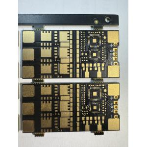
Product Description:
HD PCB (High Density PCB) is an advanced type of printed circuit board designed for high component density, miniaturization, and high-performance electronic devices.Compared to traditional PCBs, it features ultra-fine copper traces (line widths/spacings usually ≤ 0.1mm, even down to 0.03mm), tiny microvias (diameter ≤ 0.15mm, in blind/buried/stacked designs), and more layers (often 8–40+ layers). It also uses specialized materials (e.g., high-heat-resistant high-Tg FR-4, flexible polyimide) and strict manufacturing precision to support dense component mounting (e.g., fine-pitch chips).Widely used in smartphones, wearables, EVs, medical implants, and 5G equipment, it enables smaller device sizes, stable high-speed signal transmission, and reliable operation in harsh environments.
Advantages :
1. Enables device miniaturization: Ultra-fine traces, microvias, and multi-layer designs let more components fit in small spaces, supporting slim/portable devices (e.g., smartwatches, thin smartphones).
2. Boosts signal performance: Low-loss materials and short microvia paths reduce signal interference and weakening, critical for high-speed/high-frequency devices (e.g., 5G modems, LiDAR).
3. Enhances reliability: Fewer connectors (replacing multiple traditional PCBs) and harsh-environment-resistant substrates (e.g., high-Tg FR-4) lower failure risks, suitable for autos/aerospace.
4. Frees up design flexibility: Supports flexible structures (foldable phones) and stacked components (e.g., memory on CPU), easing integration of complex functions.
5. Cuts long-term costs: Though upfront manufacturing is pricier, smaller device size, fewer assembly steps, and less maintenance reduce overall expenses.
Technical Parameters:
| Min. Hole Size |
0.1mm |
| Impedance Control |
±10% |
| Board Size |
Customized |
| Surface Finish |
HASL, ENIG, OSP |
| Layer |
12L |
| Min. Line Width/Spacing |
0.075mm/0.075mm |
| Thickness |
1.2mm |
| Minimum Via Dia |
0.2mm |
| Min. Order Quantity |
5㎡ |
| Layer Count |
1-30 |
Applications:
The High Density PCB, originating from China, is a versatile product suitable for a wide range of applications due to its high-quality construction and advanced features. With a board size of 600X100mm and 12 layers, this PCB offers exceptional performance in various scenarios.
One of the key attributes of the High Density PCB is its excellent Signal Integrity (SI), making it ideal for applications where maintaining signal integrity is crucial. The carefully designed layout and high-density interconnects ensure reliable signal transmission, making it suitable for high-speed and sensitive electronic devices.
Another standout feature of the High Density PCB is its use of Staggered Vias, which help optimize signal routing and reduce interference. This design element further enhances the SI capabilities of the PCB, making it a preferred choice for complex circuit designs.
With a board thickness ranging from 0.2mm to 2.0mm, the High Density PCB offers flexibility in design and application. The 8-layer construction, featuring 2oz copper on the outer layers and 1oz copper on the inner layers, provides excellent thermal performance and reliability.
The High Density PCB is suitable for a variety of product application occasions, including but not limited to:
- Telecommunications equipment
- Medical devices
- Automotive electronics
- Industrial control systems
- Aerospace technology
Whether you require high-speed data processing, precise signal transmission, or reliable power distribution, the High Density PCB offers the performance and durability needed for demanding applications. Trust in the quality and innovation of this product to meet your specific requirements.
How is the manufacturing process of HDPCB?1.Substrate & Pre-treatment: Traditional PCBs use low-cost standard FR-4 (low Tg); HDPCBs adopt high-performance materials (high-Tg FR-4, polyimide, PTFE) with pre-treatment (e.g., plasma cleaning) for better adhesion and environmental resistance.
2. Trace Patterning: Traditional PCBs use standard photolithography for ≥0.15mm traces; HDPCBs rely on high-resolution laser direct imaging (LDI) to make ≤0.03mm fine traces, with thinner copper layers (0.5–1 oz) and precise micro-etching.
3. Via Drilling: Traditional PCBs use mechanical drilling for ≥0.2mm through-holes; HDPCBs use laser drilling to create ≤0.15mm microvias (blind/buried/stacked), saving space.
4. Layer Lamination: Traditional PCBs laminate 2–4 layers with loose alignment (≥0.05mm); HDPCBs bond 8–40+ layers via high-precision alignment (≤0.01mm) and controlled heat/pressure to avoid warping.
5. Component Mounting: Traditional PCBs use through-hole mounting or standard SMT (≥0.8mm pitch); HDPCBs use fine-pitch SMT (≤0.5mm pitch) with high-accuracy placement machines, plus nitrogen reflow to prevent solder defects.
6. QC: Traditional PCBs use basic AOI; HDPCBs add 3D AOI, X-ray inspection (for microvias), and signal integrity testing to detect tiny defects.